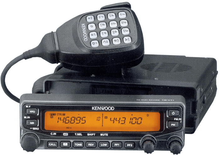
Kenwood TM-V71A Dual Band Transceiver
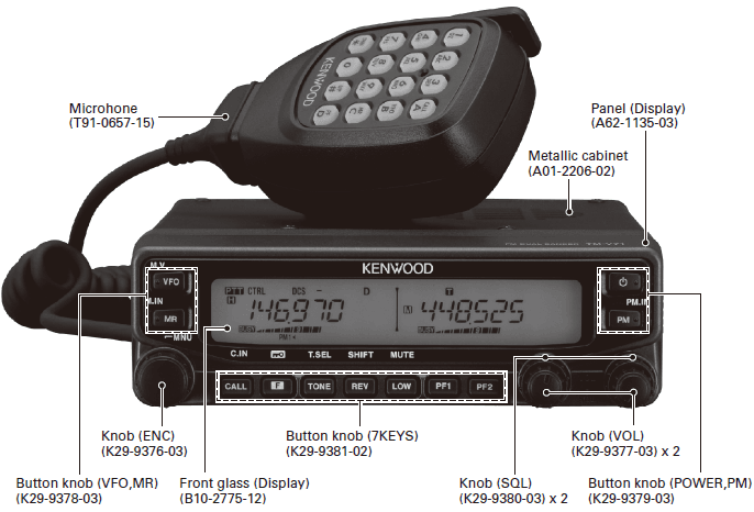
Parts and Description
DISASSEMBLY FOR REPAIR
Precautions for Disassembly
When removing the rear case from the panel, open the bottom side slowly so as not to stress the FPC, as the FPC on the rear case is connected with the connector of the display PCB.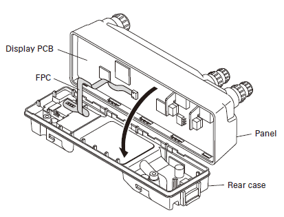
CIRCUIT DESCRIPTION
Frequency Configuration
The TM-V71A/V71E has an individual VCO and PLL unit for both band A and band B. Using these separate VCO and PLL circuits, it can receive 2 separate bands at the same time. You can also perform full-duplex operation. The band A VCO is used for the following functions:
- VHF/UHF transmission
- The first local oscillator for the band A (VHF) reception.
- The first local oscillator for the band A (UHF) reception.
The band B VCO is used for the following functions:
- VHF/UHF transmission
- The first local oscillator for the band B (VHF) reception.
- The first local oscillator for the band B (UHF) reception.
The PLL reference frequency is generated by a 12.8 MHz (band A) and a 16.8 MHz (band B) crystal oscillator connected to the band A and band B PLL ICs. This reference frequency is used for both PLL circuits. The 45.505 MHz second local oscillator for band A is generated by the FM IC crystal oscillator circuit. The second local oscillator for the band B uses the tripled 16.8 MHz reference oscillator frequency.
Note:
The PCB layout and the mounting parts are the same for the band A VCO (X57-731 B/6) and band B VCO (X57-731 C/6), although the PCB silk print is different.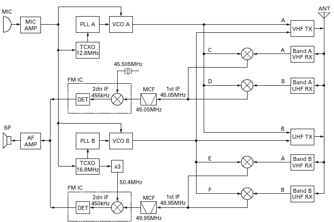
Receiver System
Band A VHF Receiver Circuit
The incoming signal from the antenna passes through a filter circuit and goes to the RF amplifier (Q228). The amplified signal enters the band-pass filter. After the signal passes through the band-pass filter, it is amplified by another RF amplifier (Q227) and then passes through the band-pass filter before entering the mixer (Q226). The frequency of the signal is converted by the first local oscillator (Upper heterodyne) to generate a 45.05 MHz first IF signal. The signal passes through the MCF (XF486), is amplified by the IF amplifier (Q495), and then enters the FM IC (IC486). The signal is converted to the 455 kHz second IF signal by the second local oscillator (Upper heterodyne). It is then detected to generate an audio signal.
Band B VHF Receiver Circuit
The incoming signal from the antenna passes through a filter circuit and goes to the RF amplifier (Q293). The amplified signal passes through the band-pass filter and is amplified by another RF amplifier (Q292). It then passes through the band-pass filter and goes to the mixer (Q291). The frequency of the signal is converted by the first local oscillator (Upper heterodyne) to generate a 49.95 MHz first IF signal. The signal passes through the MCF (XF546), is amplified by the IF amplifier (Q551), and then enters the FM IC (IC546). The signal is then converted to a 450 kHz second IF signal by the second local oscillator, which is tripled to 16.8 MHz (Upper heterodyne). It is then detected to generate an audio signal.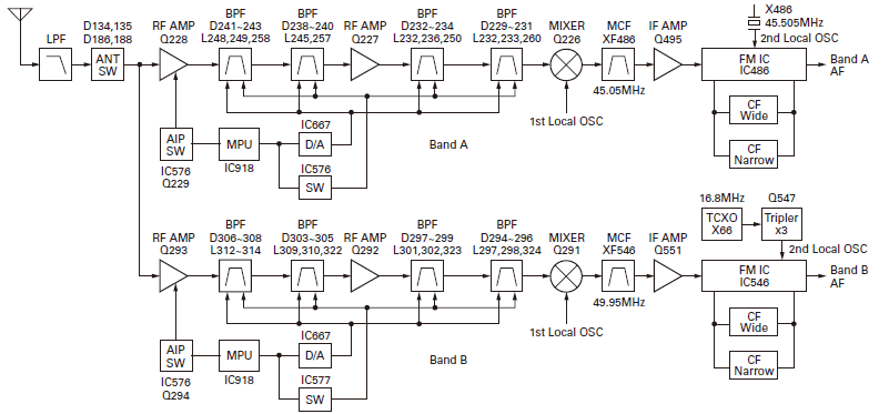
Band A UHF Receiver Circuit
The incoming signal from the antenna passes through a filter circuit and goes to the RF amplifier (Q363). The amplified signal enters the band-pass filter. After the signal passes through the band-pass filter, it is amplified by another RF amplifier (Q362) and then passes through the band-pass filter before entering the mixer (Q361). The frequency of the signal is converted by the first local oscillator (Lower heterodyne) to generate a 45.05 MHz first IF signal. The signal passes through the MCF (XF486), is amplified by the IF amplifier (Q495), and then enters the FM IC (IC486). The signal is converted to the 455 kHz second IF signal by the second local oscillator (Upper heterodyne). It is then detected to generate an audio signal.
Band B UHF Receiver Circuit
The incoming signal from the antenna passes through a filter circuit and goes to the RF amplifier (Q408). The amplified signal passes through the band-pass filter and is amplified by another RF amplifier (Q407). It then passes through the band-pass filter and goes to the mixer (Q406). The frequency of the signal is converted by the first local oscillator (Lower heterodyne) to generate a 49.95 MHz first IF signal. The signal passes through the MCF (XF546), is amplified by the IF amplifier (Q551), and then enters the FM IC (IC546). The signal is then converted to the 450 kHz second IF signal by the second local oscillator, which is tripled to 16.8 MHz (Upper heterodyne). It is then detected to generate an audio signal.
The VHF/ UHF band-pass filter is tuned to the desired frequency according to the BPF voltage output from the D/A IC (IC667), and is controlled by the MPU (IC918) and the varicap.
Transmitter System
Modulation Circuit
The audio modulation input from the microphone is amplified by IC802. After the DTMF signal and 1750Hz tone signal generated by the MPU are switched with IC806, they are mixed by IC803. After the signal is amplified by IC802 is switched by IC806, it is amplified by IC803. The signal is then pre-emphasized by Q805 and Q808, and its level is adjusted by IC804. The resulting signal goes to each of the band A and band B VCOs as a modulation signal. The TONE/ DCS signal generated by the MPU is fed to IC803. The signal amplified by IC803 is distributed, and the level is adjusted by IC804. The modulating signal goes to each of the band A and band B VCOs and the reference oscillation circuit.
Transmitter Circuit
The VHF VCO output is amplified by the RF amplifier (Q644) and driver amplifier (Q131). It is further amplified to the final output by the power module (IC131). The output signal passes through the antenna switch (D134, D135) and a low-pass filter, and is then fed to the antenna. The UHF VCO output is amplified by the RF amplifier (Q161) and the driver amplifier (Q162). It is further amplified to the final output by the power module (IC161). The signal passes through the antenna switch (D164, D165), a low-pass and high-pass filter, and is then fed to the antenna.
APC Circuit
The Automatic Transmission Power Control (APC) circuit has a differential amplifier (IC187) that compares the DC voltage generated by detecting part of the transmission output using diodes (D191, D192) with the reference voltage output from the D/A IC (IC667). The output signal is switched by IC186 and is fed to the power module of each VHF/UHF to keep the transmission output constant.
Overheating Protection Circuit
To protect thermal destruction of the power modules (IC131, IC161), the voltage of the thermistors (TH131, TH161) near the power modules (IC131, IC161) is monitored by the MPU (IC918). If their temperature becomes too high, this circuit reduces the APC voltage to cool down the temperature.
PLL Circuit
Reference Oscillator Circuit
Band A divides 12.8MHz inside the PLL IC (IC1) or band B divides 16.8MHz inside the PLL IC (IC66) to generate a 5kHz or 6.25kHz reference frequency. The 16.8MHz signal on the IC66 side is tripled by Q547 to obtain the second local oscillator for band B. The reference oscillation circuit is also modulated to improve the modulation characteristics of the DCS and 9600bps packet signal when it is transmitted.
Phase Comparator
Part of the band A VCO output is amplified by Q5 and goes to the PLL IC (IC1). Also, a part of the band B VCO output is amplified by Q70 and goes to the PLL IC (IC66). The pulse-swallow type PLL IC divides the input VCO oscillator frequency using the data from the MPU (IC918). It compares its phase with that of the reference frequency to enable the PLL synthesizer to generate the desired step.
Lock Voltage (VCO Control Voltage)
The phase differential comparator, output from the PLL IC, results in a phase difference pulse. As for the result of phase comparison with the PLL IC, a phase difference is output as a pulse. This pulse is amplified by a charge pump (Q2, Q3, or Q67, Q68) and the ripples are removed by a low-pass filter, then the signal is supplied as the oscillator frequency control voltage for each VCO.
Unlock Detection Circuit
When the PLL is unlocked, a low state voltage is output from the LD terminal (pin 8) of the PLL IC. This signal is monitored by the MPU (IC918) to control transmission/ reception switching timing.
Power Supply Circuit
Microcomputers and Peripheral Circuits
Reset and Backup Circuits
The MPU reset signal detects a rising edge of the M5 line voltage with the reset IC (IC920). When the voltage supplied to the transceiver decreases and the B line voltage falls below the detection voltage of the voltage detection IC (IC919), the MPU (IC918) detects it through the interrupt terminal, stores the data in the EEPROM (IC916), and shuts the power off.
Voltage Detection Processing
The MPU (IC918) monitors and processes various voltage statuses at the A/D ports of IC918. The squelch voltage is input from the FM IC, and a change in the noise voltage is detected to control squelch. The S-meter voltage is input from the FM IC to control the S-meter display. The thermistor voltage (temperature) is also detected through the A/D port.
Serial Control
The MPU (IC918) controls the panel section (Display unit X54-359) through synchronous serial communications.
Narrow/ Wide Switching Circuit
On band A, the receiver bandwidth can be switched between narrow and wide by selecting IF ceramic filters CF487 (Narrow) and CF486 (Wide) with a switching circuit (Q486, Q487, D486, D487). On band B, the receiver bandwidth can also be switched between narrow and wide by selecting IF ceramic filter CF547 (Narrow) and CF546 (Wide) with a switching circuit (Q546, Q548, D546, D547). The transmitter deviation can be switched between narrow and wide by setting the electronic variable resistor (IC804) on the deviation adjustment point. It is controlled from the MPU (IC918).
AF Signal System
Beep Circuit and Mute Circuit
A beep sound is generated by the MPU (IC918) and goes to cross cross-point switch (IC806). This signal is switched by the cross-point switch and is input to the electronic volume (IC804). While the beep signal is output from the MPU, audio signals for each band are muted by the cross-point switch with the serial data from the MPU (IC918). The beep signal that has had its level adjusted by an electronic volume is input to the AF amplifier (IC801).
Speaker Switching Circuit
There are two speaker jacks, J801 (SP1) and J802 (SP2). The AF signals can be output in various combinations matching the internal speakers. When an external speaker is not connected to J802 (SP2), the J802 signal is added to the AF amplifier input of SP1 via the ATT circuit and is output through J801 (SP1). When an external speaker is connected to J802 (SP2), it is output separately from the speaker for the A/B band. The crossing point switch connection can be switched by switching the menu between MODE 1 and 2, and the connection of SP1 and SP2.
Microphone Key Input
When the MC-59 (Supplied microphone) is used
The pulse is output from the CM terminal of the MPU to the microphone. The MPU judges which key was pressed from the number of pulses returned from the microphone.
When the MC-45 (Optional microphone) is used
The microphone UP/DOWN and function keys are connected to the microprocessor’s analog input. The voltage when a key is ON operates the corresponding function.
Data Terminal and Peripheral Circuits
J607 (Data terminal) is the data communications terminal on the rear of the transceiver. It handles transmission control, data input/ output, and squelch signals. There are two data communications modes: 9600 bps mode and 1200 bps mode. 9600 bps mode communications are GMSK and G3RUH packet communications. Unlike with 1200bps AFSK, with this type of high-speed modulation, Frequency modulation is carried out after the digital baseband signals (rectangular wave) are passed through a band-limiting filter. For 9600bps GMSK, for example, compared to 4800Hz signals (nearly sine wave signals passed through a filter), the signals have a hissing sound like digital modulation when listened to by ear. Different types of modulation, such as GMSK and G3RUH, are distinguished by the type of band-limiting filter used.
Transmission Signals
Transmission modulation signals enter from the PKD of the data terminals (J607). The path to the modulation depends on whether communications are set for 1200bps or 9600bps mode.
For 1200bps mode, the transmission modulation signals pass through the analog switch (IC803) and are input to IC801 (Pin 6). The signals pass through the pre-emphasis (Q801, Q802), are adjusted by the electronic volume, and are input to the VCO.
For 9600 bps mode, the transmission modulation signals pass through IC803 and are amplified by the tone amp (IC802). Signals are then adjusted by the electronic volume and are input to the VCO.
The frequency shift depends on the input signal level, so there is an amplitude limiting circuit (D702, D703) to hold the signal below 4 Vp-p to avoid extreme shifts. This circuit ensures that the PKD signal does not go above 4 Vp-p and there is no extreme frequency shift fluctuation.
Reception Signals
PR9 is the 9600 bps data communications reception output. It sends the FM detection circuit output (RD signals) through a buffer amplifier (Q607). These signals are always output, whether the squelch is open or closed. PR1 is the 1200 bps data communications reception output. It sends the FM detection circuit output (RA signals) through a buffer amplifier (Q606). The output is controlled with the cross-point switch (IC806) according to whether the squelch is open or closed.
PR1: The audio signal that was de-emphasised is switched by the cross-point switch and passed through the electronic volume. The signal is then buffered by Q606 and is sent to the data output terminal. The PR1 signal is output when the squelch is open.
PR9: The signal switched through IC666 is buffered by Q607 and is sent to the data output terminal.
Squelch Signal Output Circuit
The squelch circuits are input to the TNC to prevent conflicts from occurring between simultaneous receive mode and transmit mode traffic during packet communications (only during 1200bps). The SQC signal is output by the MPU (IC918). The SQC output can be set to the following using the menu mode.
An initial value is Busy. TX. The logic of the output is Hi active. The logic of the output can change by MCP-2A.
OPTIONAL ACCESSORIES
DFK-3D (Detachable Front Panel Kit (3 m))
External View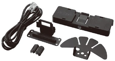
MC-59 (Keypad Microphone)
External View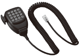
Cord Assembly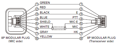
PG-5F (Extension Cable Kit (4 m))
External View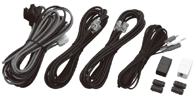
PG-5G (Programming Interface Cable (2 m))
External View
PG-5H (PC Interface Cable Kit (2 m))
External View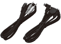
For more Manuals by Kenwood, visit ManualsLibraryy
Kenwood TM-V71A Dual Band Transceiver-FAQs
What bands does the Kenwood TM-V71A support?
The TM-V71A supports dual-band operation on VHF (144 MHz) and UHF (430 MHz) frequencies, allowing communication on two bands simultaneously.
Can I use the TM-V71A as a cross-band repeater?
Yes, the TM-V71A features a built-in cross-band repeater function, enabling it to receive on one band and transmit on another.
How do I program frequencies into the TM-V71A?
Frequencies can be programmed manually through the front panel or by using Kenwood’s programming software with a compatible cable.
What is the power output of the TM-V71A?
The radio offers three selectable power levels: High (50W), Medium (10W), and Low (5W), depending on your communication needs.
Does the TM-V71A have memory channels?
Yes, it comes with 1,000 memory channels for storing frequencies, names, tones, and other settings for quick access.
Is the display customizable?
Yes, the TM-V71A features a large backlit display with adjustable colors and brightness, allowing for better visibility and customization.
How do I switch between bands on the radio?
You can switch between VHF and UHF bands by pressing the [A/B] button on the front panel to toggle the active side.
Can I use the TM-V71A in a vehicle?
Yes, it’s designed for mobile use and includes a mounting bracket, detachable front panel, and remote head mounting options for in-vehicle installation.
What tone functions are supported?
The radio supports CTCSS, DCS, and tone burst functions for accessing repeaters and managing group communication.


